The ACE
One board, one computer, everything on it — including the keyboard. The ACE is a big board, about as tall as a Commodore 128 and a little narrower, and the front two-thirds of it is a full mechanical keyboard soldered straight to the PCB. No cards to fit, no expansion decisions to make.
The tour
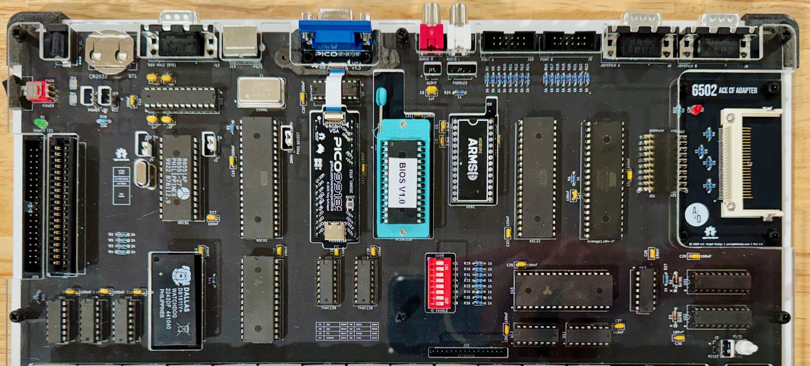
The big chip in the middle is a W65C02S — the processor. It's a 1970s design still in production today, running here at 1 or 2 MHz. That sounds slow. It is slow. It's also completely comprehensible, which is the point: there is nothing happening inside the ACE that you can't eventually understand.
Next to it, two 32 KB chips. One is RAM (what your programs live in while they run); one is ROM, holding the BIOS — BASIC, the Kernal routines that drive everything else, and a copy of the Apple I's Wozmon. There's another half a megabyte of RAM on board as well, reached a slice at a time when a program needs more room than BASIC's 32 KB.
The little black module near the video connector is the video card: a PICO9918 PRO running 6502-PICOVDP firmware, a video chip written for this family and driving a plain VGA monitor. That's where the 40×24 text screen comes from, with a color of its own for every character. Underneath the text it has four screen layouts up to 320×240, 256 colors on screen out of 4,096, two layers that scroll independently and 64 sprites — and a program written for the text and simplest graphics modes of the TMS9918A, the ColecoVision and MSX chip it grew out of, still runs on it.
The socketed 28-pin chip is an ARMSID — a drop-in replacement for the MOS 6581, the sound chip from the Commodore 64. Three voices, real filters, RCA output to any powered speaker.
The keys are 67 Cherry MX switches in a proper typing layout, wired as a matrix straight into the board. This is your keyboard; nothing needs plugging in. See The keyboard for the handful of keys that do something out of the ordinary.
The card edge behind the keyboard, standing up rather than facing out, is the cartridge slot. Cartridges drop into it from above. It's also where the KIM keypad boards go.
Round the edges: a VGA connector, RCA audio, two joystick ports, a DB9 serial port, a CompactFlash slot on its own little adapter board, a PS/2 socket, and a 5 V barrel jack.
Two switches worth knowing. The power switch does what it says. The reset button sits just above the Esc key, where you can reach it without looking — and it is not the same as switching off:
- Reset restarts BASIC but keeps your program. The header comes back, the variables start from nothing, and
LISTshows the program still there. Use it to get out of anything. - Power off, then on is the clean slate. Memory is cleared and BASIC starts from scratch.
What the other chips do
A 65C22 VIA handles the joysticks and general-purpose I/O. A 65C51 ACIA with a MAX238 next to it drives the serial port. A DS1511Y keeps the time and date when the power's off, and hangs on to 256 bytes of memory for you. An ATmega1284P scans the keyboard and hands keystrokes to the 65C02 — it also holds the CPU in reset for a quarter of a second at power-on, which is why the machine comes up cleanly instead of mid-thought.
The jumper and the DIP switches
J1 PHI2 SELECT picks the CPU speed: 1 MHz or 2 MHz. 1 MHz is the safe default and the speed everything in this guide assumes. 2 MHz is free performance if your particular set of chips is happy with it — try it, and move the jumper back if anything gets flaky.
The eight-way DIP switch marked IO ENABLE has one position for each of the machine's eight I/O sections — banked RAM, clock, storage, serial, joysticks, sound, video. Leave them all on. They're there for fault-finding: switch a section off and the ACE boots without it, which is a quick way to work out which part is misbehaving.
What's on the board
| Part of the machine | Chip | Notes |
|---|---|---|
| CPU | W65C02S | 1 or 2 MHz, jumper-selectable (J1 PHI2 SELECT) |
| RAM | 62256 | 32 KB SRAM |
| Banked RAM | AS6C4008 | 512 KB, reached a 1 KB window at a time |
| ROM | 28C256 | 32 KB EEPROM |
| Storage | ACE CF Adapter | CompactFlash in 8-bit True IDE mode, via the ACE CF Adapter on the Storage header |
| Video | PICO9918 PRO v2.0 | 6502-PICOVDP firmware: VGA 640×480, text and tile modes up to 320×240, 256 colors from 4,096, two layers, 64 sprites |
| Audio | ARMSID | 3-voice SID emulation, RCA output |
| Serial | 65C51 ACIA + MAX238 | RS-232 via DB9, 50–19200 baud |
| GPIO | 65C22 VIA | 20 GPIO pins, 2× 16-bit timers, shift register |
| RTC | DS1511Y | Battery-backed clock and 256 bytes of NVRAM |
| Keyboard controller | ATmega1284P | Runs AB Controller firmware |
| Input | PS/2 connector + 8×8 matrix header | Both live at once |
| Joysticks | 2× Atari 2600-compatible | J6 JOYSTICK A on VIA PORT A reads as JOY(2); J8 JOYSTICK B on VIA PORT B reads as JOY(1) |
| Clock | 16 MHz DIP-14 oscillator (X1) | Drives the ATmega1284 at 16 MHz and the 65C02 at 1 or 2 MHz via a 74HC163 divider |
| Reset | SW70 | Manual reset into the ATmega1284, which also provides power-on reset to the 65C02 |
| Power | 5 V DC barrel jack |
Building one yourself
The ACE is open hardware — the KiCad project, the bill of materials and the production files are all in the 6502-ACE repository. A few things worth knowing before you order boards:
- The ACE CF Adapter is a separate small board that plugs into the Storage header — part of the machine, but its own PCB and its own BOM.
- Rev 1.0 boards need the ACE RAM Patch for the banked SRAM to latch reliably. Rev 1.1 fixes it on the board.
- The video card is a PICO9918 PRO v2.0 flashed with 6502-PICOVDP firmware. The earlier Pico9918 boards, built on the RP2040, cannot run that firmware; an ACE fitted with one runs BIOS 1.6.
Board revisions to date:
- ACE Board Rev 1.1 — Fixes the LOADL/LOADH latch-enable gating for the banked SRAM: the final NAND stage becomes a NOR (LOADL = NOR(SEL_L, WB)), added as one 74HC02 (U23). Pull-ups R1–R4 and R25 go from 1 kΩ to 10 kΩ; C31 (10 µF) added at the power input. No firmware change.
- ACE Board Rev 1.0 — Initial release. Banked RAM does not latch reliably — needs the ACE RAM Patch.
📄 6502-ACE card — this chapter, the memory map and the first things to type, on two printable pages. The card index has the rest.
Next
Setting up — what to plug in, and in what order.